MEMORANDUM
To: Professor Tsu-Jae King,
Microlab Faculty Director
From: Bill
Flounders, Technology Manager
Subject: 2007 Year-End Report
Date: 18 January 2008
Cc: Katalin Voros, Microlab Operations
Manager
I.
Introduction
This memorandum documents my major
activities for the calendar year 2007. For the past year, I have continued two
primary functions, planning for the CITRIS Nanofabrication Center (the planned
successor facility to the Berkeley Microlab) and, technology support for the
existing Microlab. Though design planning and construction review of the new
lab have been on going for several years, 2007 was the first year in which my
activities have begun to focus upon specific equipment and transitional plans
for the Microlab move in its new home in the CITRIS building. Calendar year
2007 is the year during which the Microlab transition and migration has shifted
from immanent to imminent!
I reiterate the following
information from last year’s report and henceforth will only use the assigned
names below for the CITRIS building and the new laboratory. At the CITRIS
Research Symposium on December 14, 2006 the lead benefactors to CITRIS were
publicly announced. The leadership private investors are: Dado and Maria
Banatao (parents of 3 UC Berkeley graduates) Sehat Sutardja (EE ’85, ’88) and
Weili Dai (CS ’84); and, Pantas Sutardja (EE ’83, ’85, ’88) and Ting Chuk (EE
’85). In recognition of their major investment and support of CITRIS: The
CITRIS Headquarters Building will be Sutardja-Dai Hall. Thanks to the
commitment and vision of the Sutardja and Dai families, cofounders of Marvell
Semiconductor, the successor to the Berkeley Microlab will be the Marvell
Nanofabrication Laboratory.
II.
Technology Support of
Existing Laboratory
Ebeam
Lithography
Calendar 2007 started with an exploratory visit by Crestec
Corporation of Japan. Crestec was established in 1995 and has become an
established supplier of electron beam writing systems. They have placed systems
in over 30 national laboratories and universities and at over 45 commercial
sites. However, they have yet to place a tool in North America. The President
of Crestec, Mr. Hideyuki Ohyi, and Product Manager, Mr. Peter Wilshurst were
visiting the United States to define a partner institution to showcase Crestec
capabilities to the North American and US market. They found a receptive
audience at UC Berkeley.
The Crestec flagship nanolithography system (the 9000
series) is not only a high performance tool capable of guaranteed writing of 10
nm line widths, it is also an extremely robust tool with a unique column
enclosure enabling more realistic vibration, EMI and temperature specifications
than many competitors, and a patented beam focusing strategy which enables very
high dose with smallest spot size. The Crestec tool also provides a wide array
of software features including absolute necessities such as multiple input file
type conversion and proximity effect exposure dose adjustment routines. All
review of the Crestec tool indicated it would be an excellent choice for a
general use ebeam lithography tool in a multi user shared facility.
As important as the quality of Crestec’s tool was the
willingness of Crestec to negotiate with the Berkeley Microlab. There was
lengthy discussion between the Microlab and Crestec; in the end, it was a model
of win-win negotiation. This was not simply an extended debate over acceptable
pricing. Rather, it was an exploration of multiple combinations of purchase,
lease and shared access that enabled both parties to define a solution
compatible with their needs. After months of hard work, a purchase agreement
was in place by the end of August. Berkeley sent an engineer to Japan for an
on-site review and demonstration in December 2007 and the tool is due for delivery
and install in February 2008.
Finally, the Crestec purchase was one of the finest examples of the shared laboratory culture that the Berkeley Microlab has been fostering for decades. Fifteen faculty representing three departments and two colleges contributed to the purchase of this tool. Contributions from a faculty at another UC campus were almost included. The confidential details of the Crestec purchase will not be disclosed in this broadly distributed public document; however, any Microlab Principal Investigator may contact me for more information.
Proposal Development
- I developed several equipment and research
proposals to generate support for the existing and future operation.
Primary among these was a proposal to the National Science Foundation
Major Research Instrumentation (MRI) program. A joint proposal was
developed and offered to the Stanley Hall Biomolecular Nanotechnology
Center (BNC) through the College of Engineering Associate Dean of
Research. This proposal requested funds for 2 key tools at the BNC and 2
key tools at the Marvell Lab. The thrust of the proposal was to insure
broadest possible access of researchers from across campus to both
facilities. NSF usually welcomes requests that leverage multiple
facilities and lead to research cross fertilization. Unfortunately, the
BNC elected to submit an independent proposal to the NSF MRI program so as
to insure receipt of the full grant award.
- I developed a separate proposal for the Marvell
Lab to the NSF MRI program. The primary equipment proposed was a set of
integrated wet process stations; unique to the proposal was distinction of
cleaning stations by periodic table group numbers rather than by research
group application. Though this strategy has merit –and will be implemented
for the operation of the Marvell Lab, the proposal was still simply a
request for nanolab sinks and as such does not meet the research
requirement of the NSF program. An alternate strategy has been developed
to provide wet process stations for the Marvell Lab.
- I developed a proposal to the Intel Higher
Education Semiconductor / Nanostructures Program. This proposal requested
funds for purchase of an on-site hydrogen generator to meet the needs of a
soon to be received Applied Materials epi-silicon germanium deposition
system. This proposal was funded and insures that a key piece of
laboratory infrastructure required for support of the epi-SiGe dep system
will be available.
Process
Review & Material Compatibility
I review at least weekly new material and process requests.
Some highlights from the past year were: evaporation of indium arsenide for
energy band pinning – alternate and much safer process offered was sputter
deposition of indium antimonide. PZT sol gel deposition and curing – approved
in non-MOS clean rapid thermal anneal tool. Chitin and chitosan processing.
These are structural proteins being investigated as a novel IR sensitive MEMS
layer.
I have noticed a growing number of process questions
– especially by new BMLA members or the researchers of recently transferred
faculty members – related to “what tool is needed for what process.” This
reflects our growing lab membership and indicates the need for a more generic
tool/process overview in the Microlab manual. Together with the process
manager, I have begun to prepare tool table summaries that should enable lab
members to quickly compare the many redundant tools offered within a process
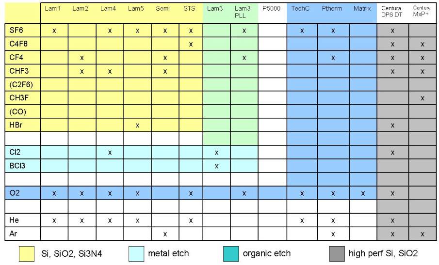
area and quickly compare them and understand the advantages of each. An example
of this type of tool table for etch processing is presented in Table 1. This is
an on going effort and will form the basis of the introductory process chapter
for the Marvell Lab on-line manual.
Staffing
The Technology Manager continues to provide direct
supervision of the BSAC Senior Development Engineer, Matt Wasilik. Matt has
successfully taken on most BSAC specific tasks previously provided by the
Technology Manager. A separate report describing his activities is included in the
Microlab Annual Report. Highlights of his report are detailed use histories and
failure analyses of the Centura and STS deep silicon etch tools; and, update on
the MEMS test structures integrated with the Berkeley Microlab baseline chip.
I served on the interview
committee for a second senior scientist for the Naofabrication Laboratory at
the Molecular Foundry at LBL. Three exceptional candidates presented seminars,
were interviewed, and received Berkeley Microlab overview/tours. This courtesy
was extended by the Molecular Foundry Nanofabrication Laboratory Director, Professor
Jeff Bokor. Ongoing coordination of the efforts at the Molecular Foundry and
the Marvell Lab are insured by this type of interaction.