MEMORANDUM
To: Katalin
Voros, Microlab Manager
From: Jimmy
Chang, Senior Development Engineer
cc: Sia
Parsa, Process Engineering Manager
Subject: 2007
Year-End Report
Date: 18 January 2008
In 2007, in addition to my regular work in process development and support, the highlights were process validation and support of Lam5 etcher upgrade, mentoring a summer intern in the project of correlating the sheet resistance and the thickness of aluminum film sputter-deposited in CPA, coordinating the production of 3 batches of show wafers for the Lam classes, and several new types of engineering test requests (ETR).
LAM5 Operation Software/Hardware Upgrade
Equipment staff upgraded Lam5
operation system to a Graphic User Interface. The upgrade included the addition
of a new computer for better user interface and enhanced recipe management. As
the result, the original on-board computer can concentrate on process/equipment
related controls. My work with this project included:
- Working with equipment staff to set up user
interface and security levels.
- Set up all standard recipes in the new interface
format.
- Validation of the etch processes to make sure
there was no process drift.
- Re-write on-line operation manual and
qualification quiz.
- Offered group training sessions for lab members
qualified for the old operation system.
Table I lists the summary results of the validation tests
after the upgrade. The main etch rate and non-uniformity are well within the
spec and the poly to oxide selective was much greater than 100. Lam5 has been
in service without any major problem related to the upgrade.
|
|
Blank
Wafer |
Patterned
Wafer |
||||
|
Main
Etch |
Main
Etch |
Over
Etch |
||||
|
Poly |
Oxide |
Poly |
Oxide |
Poly |
Oxide |
|
|
Etch Rate Å/min |
3911 |
375 |
4145 |
556 |
2848 |
20 |
|
Non-Unif. |
2.48% |
14.43% |
2.96% |
14.43% |
4.89% |
14.15% |
|
Selectivity |
10.4 |
7.5 |
143.5 |
|||
Table 1 - Lam5 Post Upgrade Process Validation Data
Correlation of Sheet Resistance and Film Thickness of Sputter-Deposited
Aluminum Film (A Summer Intern project)
In the summer, I mentored a female
high school student intern. The project I designed for her was to correlate the
sheet resistance and film thickness of aluminum film sputter-deposited in CPA.
It consisted of using most of the major tools in the Microlab. The student
learned how to use sink to clean wafers, Tystar furnace to grow thermal oxide,
CPA to sputter Aluminum film, four-point-probe to measure sheet resistance,
various photolithographic tools to pattern the film, Lam3 to etch out the
pattern, and ASIQ profiler to measure film thickness.
The program was successful. The student had an extensive
exposure to semiconductor processes and expressed strong interest in pursuing
an engineering degree in college. The correlation between sputtered Aluminum
film thickness and sheet resistance, shown in Figure 1, will be useful for the
Microlab. It can be used for a quick check of the CPA sputter deposition rate
and Lam3 etch rate without going through the tedious photolithographic
processes.
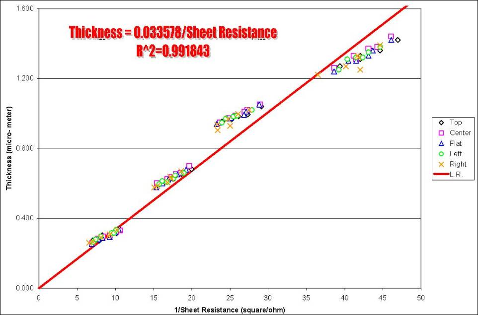
Figure 1 - Correlation of Sputtered Aluminum Film Thickness and Sheet Resistance
Show Wafers for Lam Non-Technical Staff Class
Last fall, Microlab hosts three sessions of classes for the non-technical staff of Lam Research Inc., a major equipment vendor of semiconductor industry. All the students in the class received a 6” silicon show wafer. I coordinated the process staff in production of the show wafers. It includes graphical design, mask making, thin film deposition, photolithographic patterning, etching, and wafer case selection. Thanks to all process staff, three batches, over 50 show wafers were made and delivered.
Engineering Test Requests (ETR)
In 2007, there were several new types of Engineering Test Requests in addition to the usual thin films deposition, e.g. oxide growth, poly, low stress nitride (LSN), doped/undoped low temperature oxide (LTO), and etc., in the past. They are list below.
- Lam2 etch of passivating oxide layer of III-V
compound devices for optical applications. Performed initial test runs
with satisfactory result. Then trained graduate students from UC Davis of
the process.
- AMST single-molecular layer deposition of FOTS
on packaged optical devices.
- Set up Lam5 and Ptherm for a BLMA member staff
to do special plasma characterizations and diagnosis.
- Oxford2 oxide deposition to protect manufactured
devices.
- Sophisticate wet etching on several kinds of
fused quartz samples to form multi-step surface profiles for an optical
company.
- Deposit poly-silicon films for UC Davis EE146A
laboratory class.
Support of Tystar Furnace Maintenance & Recipe Update
I have been working closely with
the equipment engineer in the area of heater calibrations, problem diagnoses,
communicate with the Tystar Company service Engineer, and final testing after
the repair.
In January, Tystar11 and Tystar12 were found to have a severe particles contamination problem. The contamination was suspected from films that contains volatile metal oxide. Changing of clean wafer boats and dummies did not solve the problem. To avoid changing the expensive quartz tube, a clean/purge process was developed to handle the problem. It consisted of a high temperature oxidation (800 ºC, 2 hours), followed by overnight pump and purge cycles with high flow of nitrogen. The cleaning process was successful and the contamination problem was solved.
Equipment Operation/Process Training
- Trained the new baseline engineer and MEMS
exchange engineer on the operations and processes of furnace, etchers, and
P5000.
- Provided semiconductor process orientation and
equipment operation training to high school summer interns.
- Trained new lab assistants (process student).
- Trained lab members on P5000 and Rudolph
Ellipsometer.
Miscellaneous
- Completed Engineering Test Requests from other
universities and research institutes.
- Changed CMP polishing head (4” &6”) when the
equipment engineer in charge was on leave or other assignment.
- Graded equipment quizzes, qualified lab members
on various tools.
- Lead monthly laboratory safety tours. Substitute
in the processing session of the orientation as needed.
- Revised the following manuals:
Chapters
5.5-6 - MOS
Clean Gate/Dry Oxidation and Annealing Atmospheric Furnace.
Chapter 5.7 - MOS Clean Annealing
Atmospheric Furnace.
Chapter 5.13 - Tystar13
Non-MOS Clean POCl3 Doping Furnace
Chapter 5.14 - Tystar14
Boron+ Doping Furnace
Chapter 5.16 - Tystar16
Non-MOS Poly-Silicon LPCVD Furnace
Chapter 5.18 - Tystar18
MOS Clean Aluminum Sintering Atmospheric Furnace
Chapter 7.5 - Lam5 Poly-Silicon TCP
Rainbow Etcher