MEMORANDUM
To: Katalin
Voros, Operations Manager
From: Kim Chan, Assistant Development
Engineer
Subject: 2007
Year-End Report
Date: 18
January 2008
cc: Sia
Parsa, Professor Andy Neureuther
This is a summary of the
activities and projects that I was involved during 2007
I.
SEMICONDUCTOR PROCESSING
I
have been working on special photoresist and lithography projects with the
Advanced Lithography Group.
- Thinned
CGR-2205 resist with PGMEA, spun coat wafers at various speed, baked,
measured thickness and R. I. Chose
to spin coat 1:3 CGR-2205 resist and ARC-600 anti-reflective coating on
wafers, baked, test exposed a wafer on ASML stepper, and developed it for
Marshal.
- Transferred
the 555A etched oxide sem picture files to Marshal. After Marshal did the EBL, I inspected
the cgr resist patterns under the microscope, took LEO SEM pictures on cgr
and zep resist patterns and printed some cgr resist patterned pictures for
Marshal. Measured oxide and zep
resist thicknesses on 3” wafer, bonded oxide/zep 3” wafer on 6” silicon
wafer with cool grease, baked, put under vacuum, etched oxide in
centura-mxp, measured oxide and zep resist thicknesses, debonded, cleaned
wafer and took sem pictures for Marshal.
Found zep resist didn’t get clean in piranha bath, but needed
scrubbing in acetone and then piranha clean again. Took oxide pattern sem pictures on LEO
again after cleaning the zep resist and transferred sem picture files to
Marshal. Checked oxide etch information and etch time, zep resist
information and sent them to Marshal.
Printed zep overview sem pictures, took more zep sem pictures,
printed and sent them to Marshal for shotnoise experimental analysis.
- Grew 300A oxide
on wafers, measured oxide thickness on nanoduv and Rudolph
ellipsometer. After Marshal did
the EBL, I inspected the thin oxide, pmma and cgr resist EBL patterned
resist under the microscope and marked the wafers for sem work. Took sem pictures on pmma, cgr, krs and
zep EBL patterned resist wafers for Marshal. Bonded 3” cgr, pmma, krs and zep resist patterned oxide
wafers on 6” Si wafers with cool grease, baked, measured oxide thickness
and put under vacuum. Etched oxide
on cgr, pmma, krs and zep EBL patterned wafers in centura-mxp, measured
oxide thickness, debonded, cleaned wafers, took sem pictures and sent them
to Marshal for shotnoise experimental analysis.
- Looked for
missing SPIE 04 mask.
I
have been working on special projects for the Microlab process group.
- Cleaned and
lubricated GCA wafer stepper 2 and 6 stage rails, cleaned and lubricated
GCA pattern generator stage rails, and made masks for the Microlab while
Marilyn Kushner was on vacation.
- Grew oxide,
deposited PECVD oxide, ran the lithography process, etched oxide in
centura-mxp and etched the silicon (pocket) wafers in TMAH and centura-dps
for the RZE, Inc. in order to
produce pinhole free, 482 µm to 508 µm deep and 4” circular pocket on 6”
wafers. First, started process
with standard I-line resist litho process on 6” oxide test and prime
wafers, exposed on ksaligner, etched oxide in centura-mxp, etched silicon
pocket in TMAH etchant and measured pocket depth. Found circular shape changed to octagonal
shape on silicon pocket, pocket was too small to fit 4” wafers and had
pinholes on pocket. Second, tried
SPR-220 resist litho process on 6” oxide wafers, exposed on ksaligner and
etched oxide in centura-mxp, partly etched silicon in centura-dps, finished
etching the silicon pocket in TMAH etchant and measured pocket depth. Found SPR-220 resist popped off the
wafer edge, sputtered onto the pocket area and prevented some oxide spots
being etched. Also found SPR-220
resist produced fine hairline cracks on oxide area during centura
etch. These fine hairline cracks
showed up on the oxide area after TMAH etch. Third, tried 2 µm I-line resist and S1818 resist litho
process on 5 µm oxide wafers, uvbake baked S1818 resist, etched oxide in centura-mxp,
partly etched silicon in centura-dps, TMAH etchant and measured
pocket depth. Found wafer edges
were thin, ragged and fragile after TMAH etch. Fourth, tried SPR-220 resist litho process on 6.35 µm oxide
6” wafers, exposed on ksaligner, hardbake some wafers for 15 hours and
more, uvbake one wafer 20 times with the “flash” recipes, etched oxide in
centura-mxp and etched silicon pocket in centura-dps. Found SPR-220 resist didn’t hold up
during the deep silicon etch step.
Fifth, tried 100 µm
negative sheet resist litho process on 6.35 µm oxide 6” wafers, used a 4”
silicon wafer as a mask to expose pocket pattern on ksaligner, etched
oxide in centura-mxp, partly etched silicon in centura-dps and finished
the silicon pocket etch in TMAH etchant.
Found silicon pocket was too small by using a 4” wafer as the
mask. Sixth, tried 100 µm negative
sheet resist litho process on 6.35 µm oxide 6” wafers, used a 4” silicon
wafer as a mask to expose pocket pattern on ksaligner, etched oxide in
centura-mxp and finished the silicon pocket etch in centura-dps. Found using 4” wafer as a mask, then
the silicon pocket turned out too small to fit a 4” wafer. Seventh, asked machine shop to make
101.5 mm, 101 mm, 100.5 mm disks and 102 mm ring metal mask set for
repeating the pocket wafer process with 100 µm negative sheet resist litho
process on 6.35 µm PECVD oxide and 2.35 µm thermal oxide 6” wafers, used a
4” silicon wafer as a mask to expose pocket pattern on ksaligner, etched
oxide in centura-mxp, finished the silicon pocket etch in centura-dps and
grew oxide to strength the pocket wafers as the final step of this
process. Finally, 101 mm and 100.5
mm disk masks produced the best fit for 4” wafers in the 6” pocket
wafers. Greg Mullins from RZE,
Inc. picked up three 100.5 mm masked pocket wafers.
- Cleaned and
tested parylene system until it worked well. Cleaned S. S. L. voltage multiplier stack in p-therm,
prepared parylene adhesion promoter and cleaned voltage multiplier stack
in it. Deposited 52 grams
parylene-c and measured the thickness for Bruce Dalen and Peter Berg from
Space Sciences Laboratory.
- Collected
PMMA process information, called Microchem Co. to check process
information, decided on process procedure, got price quote on PMMA resist
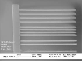
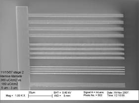
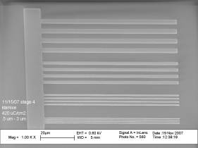
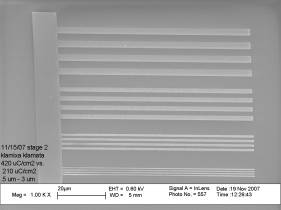
and PMMA Remover PG, calculated material and process cost. Confirmed ETR proposal, spun PMMA
resist at various spin speed to get the correct thickness, designed mask
layout, ran ebl exposure tests, exposed patterns on PMMA resist with
jeol107 sem at 18 KV and took sem pictures on the LEO sem for Dr. Yehiel
from KLA-Tencor. The following are
a few sem pictures to show the comparison of the standard exposures
and half dose/full dose exposures:
- Bonded Si to
Si wafers with cool grease for U. C. Davis a few times.
- Ran contact angle
measurement ETR on kruss.
- Assisted
Rosanna Cambie to coat AR3-600 anti-reflective coating, UV210 resist, ran
FEM, exposed Si and SOI wafers on ASML stepper, developed and inspected
them.
- Operated the
LEO SEM for Danny Xiong, took sem pictures from AMAT and sent him the sem
pictures.
- Collaborated
with Jimmy and Marilyn and made 65 Lam show wafers.
- Monitored
the phosphoric acid bath level on sink7 after the leak was fixed. Compared phosphoric acid bath
temperature reading to an external temperature thermometer. Monitored H2O drips to maintain acid
level. Checked nitride etch rate
before and after phosphoric acid evaporate.
- Showed Al
Briggs how to install the syringe properly on the Kruss system. Searched the websites for syringe
information, checked broken syringe information, related the information
to Al and tested the Kruss after it was fixed.
- Assisted a
lab member to swap wafer chuck parts on the Canon aligner, tried to focus
his sample on the aligner and went to machine shop for proper wafer chuck
screws.
- Gathered
wafer chuck dimension and vacuum grooves information on spinner1 and
svgcoat3, took pictures of wafer chucks and sent information to Dr. Y.
Gotkis from KLA-Tencor.
- Tried out
new software for matrix asher.
Processing
involved many silicon equipment and analytical instruments in the
Microlab. This year I learned how to
use the centura-dps system, flash process on uvbake system and negative sheet
resist process. Attended the wafersaw
training session and watched how to deposit FOTS film on amst system.
II.
EQUIPMENT & PROCESS MAINTENANCE
Equipment
Maintenance
- Rinsed
I-line resist line on svgcoat6 with acetone, rinsed resist bottle with
acetone, re-installed the bottle with acetone, primed the line with
acetone and kept the line soaking in acetone.
- Ran image
quality control and illumination uniformity tests on the ASML stepper.
- Tried to
solve the ASML stepper problems such as parameter out of range and lens
temperature errors.
- Ran wafers
to test the ASML stepper when there was a problem reported such as reticle
reading problem.
- Cleared the
Asyst smif pod loading and unloading problem.
- Worked with
Rite Track serviceman to see if we can resolve the resist coating defect
problem on svgcoat1 and svgcoat2.
- Checked
nanoduv reported problem.
- Checked and
cleared svgcoat6 and svgdev6 problems when needed.
- Checked and
corrected program recipes to solve problems on svgcoat1, svgcoat2,
svgcoat3 and svgdev.
- Replaced
I-line, G-line and SPR 220-7.0 photoresists on svgcoat1/2, SPR-220-7.0
photoresist on svgcoat3, I-line and UV210 photoresists on svgcoat6 and
primed the photoresist lines.
- Tried to
solve I-line resist pinhole problem after dispensing on svgcoat3.
- Assisted
David Lo to test svgdev6.
- Refilled
water in the chiller for the svgdev6 when needed.
- Disposed
resist waste and replaced new container on svgcoat6.
- Disposed
resist waste from 432c sink.
- Removed
stuck and broken wafers in Matrix chamber, restarted the matrix asher,
loaded recipe, reset heater and tested it
- Tried to
solve LEO sem focus problem and no signal input error.
- Assisted
staff on Disco saw and wafersaw.
- Assisted LEO
sem service representatives and checked LEO sem status when they were
working on it.
- Checked and
cleared gcaws6 problems such as removed stuck reticle, stage time out
error, RMS, Aldn, ACS, floppy drive, air pressure, light low and
auto-focus failure problems on gcaws6 when possible.
- Tested Sopra
ellipsometer after the software upgrade.
Checked Sopra ellipsometer log in and noise measurement problems
and measured thin oxide thickness on wafer.
- Checked
Quintel aligner problem and cleared it.
Checked jitter problem and related the problem to Phil until it was
fixed.
- Test vacuum
problems on parylene system and followed through until it was fixed.
- Checked
sink3, sink5, sink7 and svgcoat3 reported problems.
- Found
draining problem on sink7 bath and process codes changed. Changed process codes back to the
original codes. Monitored the
phosphoric acid bath level after the valve was fixed.
- Assisted
Changrui on gcaws6 while he was checking on how to back up the software in
the system. Arranged the hard
drive back up dates with Evan and Changrui. Labeled the wire connections to gcaws2 hard drive and gcaws6
Micro DFAS hard drive. Removed
gcaws2 hard drive and gave it to Changrui to clone. Tested gcaws2 and gcaws6 operations
after the hard drives were cloned.
- Tried to
assist when jeol107 sample holder was dropped into the jeol107 chamber.
- Cleaned lab,
restocked gowns and etc. for lab tour.
- Restocked
aluminum foil and cool grease in Y1.
- Tested
vacuum on spinner1.
Process Maintenance
I have been responsible to maintain general
photolithography processes for the Advanced
Photolithography Group. This
involved the following:
- Recycled
used 6” wafers.
- Piranha
cleaned beakers, graduated cylinders and small brown bottles for mixing
resists.
- Cleaned
individual wafer holders and labeled them to store 3” wafers for Marshal.
- Ran focus
tests on the asml stepper.
- Grew oxide,
measured oxide and resist thickness on nanoduv & Rudolph elllipsometer
on wafers.
- HMDS primed,
coated resists, exposed wafers, PEB, developed and inspected them.
- Inspected
wafers on the uvscope, took pictures on the uvscope and the LEO SEM when
needed.
- Checked and informed
DUV group on process data, equipment information and equipment status.
- Looked up
notes on flattened mask3 C. D. sizes, thin apex-e & thin cgr-2205
resist line width results for Marshal.
I
have been responsible to maintain part of the general photolithography
processes for the Microlab and the process group. This involved the following:
- Monitored
UV210 photoresist uniformity and thickness from svgcoat6.
- Monitored Eo
and illumination uniformity of ASML stepper using UV210 photoresist.
- Recycled
test, flat and ultra-flat silicon wafers to be used on the GCAWS6 and ASML
stepper.
- Cleaned 6”
dummy wafers for svgcoat3, svgcoat6, svgdev6 and ASML stepper.
- Prepared
photoresist coated wafers for ASML stepper field servicemen and the
process group.
- Refilled developers
on svgdev6, EBR and HMDS on svgcoat6 when I see they are low. Restocked EBR in the lobby chemical
cabinet when it was reported out
- Cleaned and
dehydration baked wafers for processing.
- HMDS primed,
coated resists, exposed wafers, PEB, developed and inspected them.
- Monitored
the photoresist inventory on 6” wafer track, labeled DUV photoresists and
stored DUV resists and AR3-600 antiflective coating in refrigerators.
- Assisted lab
members in programming on the svgcoats and coating ARC-600.
- Sorted and marked
6” dummy wafers for svgcoat3, svgcoat6, svgdev6 and ASML stepper.
- Set up LEO
sem accounts for qualify users.
- Restocked
gloves, texwipes and printer paper in the LEO room when I see they are
low.
- Informed
Susan to order UV210-0.6 resist when it is low.
- Ran F/E
matrix, system focus, microscope rotation, baseline tests and made
corrections on gcaws6.
- Tested
programs on aptchrome and asked Tom to modify them.
- Refilled
developer in aptchrome.
- Tested
emulsion exposure problem on gcapg.
Tried the emulsion mask swapping procedure as suggested by Dick
Zegra from RZE, Inc., but was unsuccessful in solving this focus problem.
- Cleaned
gcaws6 FEM mask and svgcoat6 transfer stations.
- Checked SSH
transfer client operation and file saving commands on kruss system.
- Checked the
resist lift-off procedure and searched for usaf mask information as
requested.
- Assisted Yi
Du and Linjie Zhou from U. C. Davis on the cool grease bonding process.
- Assisted
Marilyn on working a show wafer for a retiring professor.
- Transferred a
little SPR-220 resist from svgcoat1 and svgcoat2 to a dropper bottle for a
lab member. Transferred some
SPR-220 resist from svgcoat1 and svgcoat2 to svgcoat3.
- Advised
Anita Pongracz to filter the AR3-600 anti-reflective coating when she had
granular problem.
- Assisted
Anita Pongracz to mix 100:1 HF in sink7.
- Showed Antal
how to set up EKC-270 resist stripper bath.
- Showed a lab
member how to expose wafers on ksaligner manually.
- Showed lab
members how to run FEM on gcaws6.
- Added EBR
program on svgcoat3.
- Checked spin
speed and spin time on srdsink8 and looked for SVC-14 resist stripper as
requested.
- Checked
Tystar13 and vacoven information for a lab member.
- Transferred
Design CAD file to a lab member.
- Cleaned
transfer boxes for sink5, brown bottles and labware.
III.
INSTRUCTION
& DOCUMENTATION
Instruction
- Instructed
and qualified researchers on equipment operation and fabrication
procedures when necessary.
- Showed staff
how to use sink3, gcaws6 and LEO S.E.M.
- Gave lab
tours for monthly orientation when needed.
- Assisted and
showed a few lab members how to use the
-
Wafer stepper 2 & 6
-
Kruss Contact Angle
Measurement System
-
LEO S.E.M.
-
Matrix asher
-
Memscope
-
Nanoduv
Microspectrophotometer
-
Svgcoat6 and svgdev6
-
Sink432A, sink432C and
sink3
-
Sopra ellipsometer
-
UVScope
-
Vacoven
- Qualified
lab members on the operation of the
-
Canon projection aligner
-
GCA wafer stepper 6
-
Headway spinner
-
Hummer sputter system
-
Jeol107 sem
-
Kruss Contact Angle
Measurement System
-
LEO sem
-
Matrix asher
-
Nanoduv
-
Nanospec
-
Primeoven
-
Quintel aligner
-
Sinkcmp spinner
-
Sinks
-
Sopra ellipsometer
-
SVG coat and develop
systems
-
Technics-c asher
-
UVScope
-
Vacoven
-
YES prime oven
Documentation
- Wrote daily
reports to Professor Andy Neureuther.
- Wrote weekly
reports to Sia Parsa for four months.
- Wrote cmpsink
report and mask clean chapter manual.
- Revised
process module 10 to 14, canon, gcaws6, heatpulse1 & 2, kruss,
svgcoat1, svgcoat2, svgcoat3, svgcoat6 and svgdev chapter manuals, gcaws2
& gcaws6 written quizzes, svgcoat3, svgcoat6 and svgdev6 posted signs.
- Graded asiq,
cpa, disco, gcaws2, gcaws6, jeol107 SEM, lam1-3, LEO SEM, Quintel aligner,
svgcoat6, svgdev6, svgdev, sinks, wafersaw and westbond lab quizzes.
- Input the
UV210-0.6 resist thickness and Eo data into the process monitor on the
Microlab web page.
- Recorded
gcaws6 F/E matrix test and baseline correction results on log book.
- Informed DUV
researcher on the progress of the processes by sending him e-mails.
IV.
SUMMARY
I had assisted Marshal
Miller on his shotnoise experiments, so he could analyze the data. I had prepared thin photoresists for him to
do the EBL in LBL. I grew oxide on
wafers, coated with various resists, ran preliminary exposure tests, etched
thin oxide patterns on wafers after Marshal did the EBL in LBL, stripped the
resists and took SEM pictures before and after stripping the resists and after
oxide etch for Marshal to analyze the data on his shotnoise experiments. I had assisted the Advanced Lithography
Group to run the experimental process well this year.
I had completed many ETR
runs, had assisted staff and lab members to make processes run smoothly in the
Microlab. I had assisted the Microlab
to maintain equipment when necessary to keep equipment in good running
conditions and minimize equipment down time. I had graded written quizzes and
qualified lab members on equipment so the lab members could use the Microlab
facility. I had revised chapter manuals, process modules and written quizzes to
keep them updated. I had made masks
when Marilyn was away on vacation so lab members could continue their
work. I had assisted the process group
to maintain the general processes in the lab to run smoothly this year.