MEMORANDUM
To: BSAC Faculty Directors
William Flounders,
Microlab Technology Manager
From: Matthew Wasilik, BSAC,
Senior Development Engineer
Subject: 2007 Year-End Report
Date: 18 January 2008
cc:
Katalin Voros, Microlab
Manager
Professor Tsu-Jae King
Liu, Microlab Faculty Director
I have worked as a
development engineer for the Berkeley Sensor & Actuator Center for 7 ½ years. The following summarizes what I have
accomplished during the past 12 months.
I.
ENGINEERING, DESIGN, & DEVELOPMENT OF NEW EQUIPMENT
IN MICROLAB
- AMST
The
AMST is a molecular vapor deposition tool with the enhanced capacity to modify
surface layers with vacuum ultraviolet light via a special lamp assembly that I
worked to design, install and characterize previously. AMST was subject to a
fair amount of use that involved a wide range of applications in 2007.
When an expansion valve failure brought
the system down in early summer 2007, I worked to troubleshoot. AMST service
personnel attempted to diagnose the problems and provided a quotation to
replace printed circuit boards, digital controllers, and a nupro actuator. The
total cost for this exceeded $7,000.00, with a 30-day lead time. I in turn
continued investigating independently and determined the actual root cause to
be solely with a digital controller. A new PLC was ordered at a cost of
$1,500.00. In addition, I determined that the entire LINE2 valve manifold was
faulty, in contrast to AMST’s nupro failure diagnostic. The valve manifold was
replaced, and the system was brought back online in a prompt manner. I’m proud
to report having saved the lab thousands of dollars in this case, as well as
weeks equipment down time (due to AMST misdiagnosis). In addition to troubleshooting
and solving equipment failures, I provided process support to researchers on
this special equipment. A molecular vapor deposition of TEOS with subsequent
photochemical treatment w/ VUV (172 nm) irradiation to form thin, “nanoskin”
silicon oxide films at room temperature was developed and standardized for the
system. This particular process was developed for potential functionalization
of polymer substrates.
- HFvapor
Equipment
HFVAPOR
is a hydro fluoric acid vapor phase etch (HF VPE) apparatus used for
stiction-free silicon dioxide etching. Due to clamping issues with the
electrostatic chuck on this tool, I designed a new mechanical clamp specifically for a critical MEMS Exchange process
order from BSAC.
Because this new design holds wafers and dies with simple mechanical force, it
is less susceptible to malfunction. The
clamp is made of HDPE, and allows up to 45 chips to be HF vapor released at
once. The final HF release results for the MEMS Exchange run were good, and the
clamp design will serve as basis for future application specific designs.
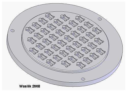
Figure 1 - Mechanical Clamp
for HF Vapor System
II.
SUSTAINING
OF EXISTING TOOLSET & SUPPLEMENTARY PROCESS DEVELOPMENT IN MICROLAB
- Centura DPS DT
Despite
the various mechanical, electrical, and consequent process issues experienced
throughout 2007 with this equipment, the DPS deep silicon etcher saw the most
use since its inception into Microlab 3 years ago. I continued to operate as
both equipment manager and process engineer for this increasingly important
tool. One major mechanical issue involved an atmospheric leak in February due
to a component failure inside the cathode assembly. Note a similar type of
failure occurred back in 2006, nearly one year to the date (see Figure 2). Both of these atmospheric
leaks resulted in large amounts of chamber downtime. Difficulty in diagnosing
this problem was complicated due to the asymmetric symptoms exhibited. Applied
Materials was made well aware of the potential for a periodic predictive leak
failure in the assembly. Their response included scheduling a preventative
maintenance plan to help obviate anticipated future problems. Further major
issues encountered with the equipment this year included an electro static chuck
power supply failure, chamber pressure control issues due to the throttling
gate valve, and RF generator power problems with both the bias and plasma
source supplies. What’s more, Microlab staff members worked in parallel to
install two additional chambers on the Centura platform this year (minimal
supervision from AMAT service). As daunting as all of this may have been, I am
pleased to report that many of these challenges were met over the course of the
year, and that system downtime was in fact minimized. A detailed report on the
state of Centura DPS processing was written and submitted to BSAC directors and
student researchers in late 2007.
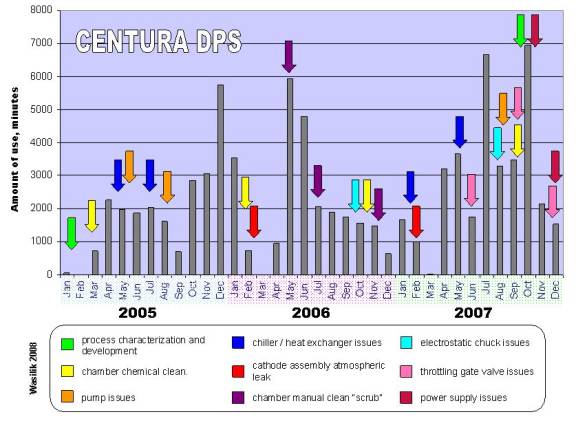
Figure 2
- Centura Use Chart vs. Problems Encountered
Dynamic process drift with DRIE process
is inherent, but the large number of mechanical and electrical problems that
have saddled Centura DPS this year have necessitated more frequent recipe
adjustments. I assisted many labmembers over the course of the year with
repairing, as well as optimizing DPS deep silicon etch recipes. Such
adjustments involve an iterative approach, with etch-and-inspect cycles,
following the path of steepest ascent along Centura DPS’ formerly characterized
response curves. Target results were usually achieved within 3-4 iterations. An
example of this may be viewed in Figure
3, where by the standard recipe profile was too reentrant and ultimately
undercut the Labmember’s silicon features. In this case I worked to adjust recipe
parameters that controlled profile taper, and was able to achieve the straight
profile shown (right side) within a few iterations.
Another
problem inherent with the Centura system lies within the software. Centura
platform software dictates a protocol that allows qualified Labmembers to write
and modify their own recipes. Unfortunately though, this has tended to lead to
more problematic etch results, as DRIE recipe programming can often be
non-trivial. What’s more, poor results are in turn usually blamed on faulty
equipment, rather than a flawed recipe. I have encouraged Labmembers to consult
with me concerning specific DRIE application needs, and will continue to assist
them in obtaining their goals. I demonstrated several times during the course of
the year that the DPS chamber was capable of producing reasonably good results,
with the right recipe, satisfactory for most applications.
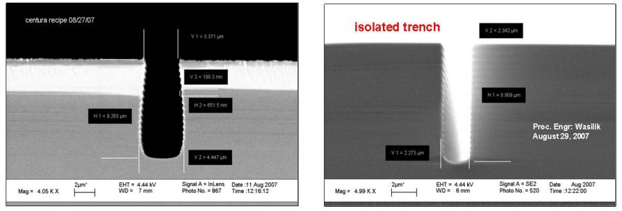
Figure 3 - LEFT:
Reentrant profile encountered using standard recipe.
RIGHT: Iterative procedure implemented to produce straight profile.
Once the upper hand is gained with
respect to physical equipment issues, a second generation design of experiment
is slated to be performed on the etch chamber. This will serve as a foundation
for implementing routine statistical process control on the DPS DT chamber. SPC
for the tool is scheduled for implementation early 2008.
- Flipchip
The Suss MicroTec FC-150 flipchip bonder is one of
the more sophisticated, high performance equipments currently residing in The
Microlab. It is capable of performing thermocompression bonding with 50kg of
force at 450°C, and holding a post-bond alignment accuracy of 3 micron or
better. I continued to serve as equipment and process support engineer on this
equipment in 2007. Due to some of the
User-error mishaps encountered with expensive silicon carbide tooling
previously, a more rigorous training system was implemented for this system in
2007. This regimented training has succeeded in reducing labmember related
problems on the tool.
The
FC150 equipment was not without its own mechanical and electrical failures in
2007. I continuously worked to troubleshoot, determine root cause, recommend,
and offer cost effective solutions in dealing with these problems as they
occurred. At the beginning of the year, I specified and oversaw the
installation of a new 6 inch chuck for this equipment. The chuck tooling was
part of the original donation from IBM, and the upgrade gave our system
capacity to bond single dies to others dies, 4 inch, 5 inch, or 6 inch wafers.
However, soon after the upgrade a severe rotational misalignment error issue
was noted. After investigating, the problem was found to be with a “theta”
tension spring in the new 6inch chuck. The old spring was plastically deformed.
I outlined a path to have a special replacement spring fabricated, to save lead
time and money. The spring stock was specified and ordered, but in the end we
simply used the spring from the old 2 inch chuck. I assisted machine shop
personnel during its installation. Proper spring function was verified, and the
rotational error issue was confirmed solved. Spending substantial time with
this equipment has further allowed me to gain a more in- depth knowledge of the
OS-9 software and built-in service routines that are needed to properly sustain
and troubleshoot the equipment. Problems with relays, vacuum valves, and
software coefficient settings for robots were addressed continuously over the
year as they arose. System calibrations were performed on FC150 as needed.
SET
(Smart Equipment Technology) re-acquired Suss’ flipchip tooling division in
2007, which our FC150 falls under. After the official transfer, I participated
in meeting with SET representatives to discuss status of our flipchip. The
laser leveling option with our system was previously determined to be
non-functional due to a failed laser. SET proposed a discrete component
replacement plan regarding this, which was more cost effective than a previous
“black-box” replacement scheme. I will look forward to working with SET and
this equipment in future. I provided process consultation and enhanced
equipment capability overview for all flipchip-qualified Labmembers as needed.
Specific equipment engineering, calibration, and operations training was also
provided for Microlab staff engineer Danny Pestal, earlier in the year. An
updated flipchip operations lab manual was completed and posted online. I’m
please to report that perseverance with this system has paid off: flipchip is
currently being used with good results.
- STS
STS continues
to be a deep reactive ion etch workhorse for the Microlab. It was used 160
hours (9566 minutes) per month on average this past year, an increase from
previous years’ averages. Aside from routine training and qualifications on the tool,
I provided process support for researchers and staff members alike. In
particular I worked to redevelop and fine-tune recipes for a critical MEMS
Exchange process run for Professor Lin’s group. I trained and qualified the
MEMS Exchange’s resident process engineer, then assisted with meeting target
requirements: excellent mask selectivity (>100:1), smooth sidewalls, no mask
undercut, and capability to stop on oxide without footing. All of these process
goals were achieved with one recipe after only a few iterations.
I
continuously worked to sustain DRIE processes at STS this past year. Dispelling
process misinformation among researchers, educating labmembers on the specifics
of DRIE process drift as necessary, and continuing recipe development and
process support was key to upholding 10,000 minutes (average) of use per month.
Process drift for DRIE processes is inevitable. The main cause for this is
thought to be carbon-rich byproduct (sputtered resist, passivation gas deposition step, etc.)
accumulation on the chamber walls over time. This buildup changes plasma
chemistry, and results in a net reduced fluorine availability. Process drift at
STS occurs in cycles. Typically Microlab’s STS chamber experiences 3 etch
regimes over a six month period. The first stage follows a clean ceramics
install, and is characterized by aggressive, reentrant profile etches. A
moderately used chamber defines the second stage, most recipes in STS database
were developed for this regime. The third and final stage of the chamber is
distinguished by lessened etch rates and etch “energy”. This is due to lessened
available reactant, but recipes may still be adjusted to produce same results
as previous. At the end of the third stage mechanically cleaned ceramics are
installed, and the cycle repeats. Note each regime requires its own tuned
recipes for optimal results. A premature third stage condition was encountered
at STS this past year. I worked to support researchers in modifying recipes and
verifying results inside this third stage etch regime. Note several critical
etches were developed herein this third stage, thus an early ceramic install
was not an option (e.g. Professor Lin’s MEMS Exchange SOI etch described
previously.) The cause of the premature
third stage regime at STS is still under review.
I
proposed reinstating a baseline monitor for STS (and Centura-DPS DRIE) to
Microlab Management in 2007. The monitor was approved and such will allow
process staff to determine which stage chamber is etching in, and allow for
quicker recipe recommendations and adjustments if necessary. I designed a new 4 inch contact
mask and had it made in The Microlab. Upon request, I provided a copy of this
new mask layout to Dr. Frank Yaghmaie, Northern California Nanotechnology
Center, University of California Davis. I had worked to assist BSAC at Davis
with their Alcatel DRIE process formerly. Statistical process control charts
were also developed for the monitor, which will be instated early 2008.
III.
PROJECTS
- Kodak
Process Development
I
worked on a lengthy, process run for Kodak, BSAC industrial affiliate, in early
2007. I agreed to perform process work for this project due to an anticipated
subsequent, and substantial funding for BSAC. The process work consisted of
developing a process flow (Figure 4),
troubleshooting and repairing the original CAD feature layout, submitting masks
for fabrication, lithography, DRIE through etch, and bonding. I encountered
many challenges with the process during its course, but managed to provide
Kodak with working devices. Follow up meetings with Kodak confirmed this,
status of funding however still unclear. A detailed, comprehensive report with
recommendations for future processes was written and submitted to BSAC
directors and student researchers involved with the project.
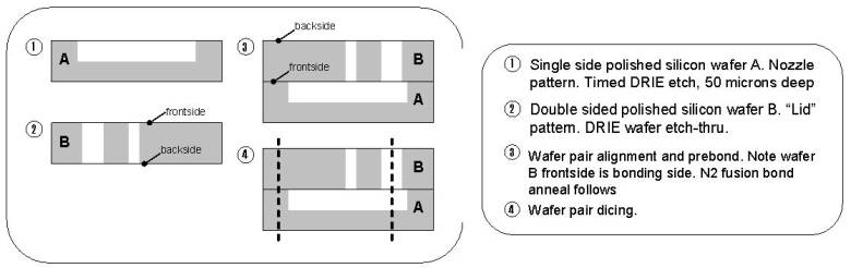
Figure 4 - Kodak Basic
Process Flow and Description
- OXFORD2
Pedestal Heater: Failure Analysis & Redesign
The Oxford2 PECVD equipment experienced
a failure with its wafer pedestal heater in October 2006. This pedestal
essentially served to hold the substrate at the correct height under a plasma
while heating the wafer in a vacuum. A vacuum sealing weldement on the pedestal
was found to have had failed, which disallowed any further processing. I became
involved in the redesign of the pedestal, but first worked to understand the
original cause of failure. Through investigative analysis I found that
surprisingly, under normal operating conditions, the original pedestal design
was doomed to fail! With this in mind,
I worked to engineer and design a completely new pedestal, operating under a
list of functional requirements. I used Solidworks, AutoCAD, and MathCAD to
design the new system. This work ran over into early 2007. The assembly was
fabricated in the Cory Hall Machine Shop, and the new pedestal heater assembly
was installed in 2007. A schematic of the components that I designed may be
viewed in Figure 5.
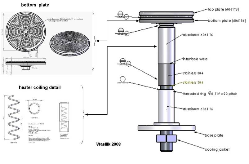
Figure 5 - Custom Mechanical
Design Elements: Oxford II Pedestal Heater
- Liftoff Process
Development
I
investigated several standard and non-standard lift-off methods, documented and
reported the results for the bi-annual BSAC industrial advisory board meeting.
The project’s main goal was to study, verify, and recommend one or more
lift-off methods for incorporation into a standard Micro lab process module.
Defining a baseline lift-off process for use by a large group of researchers
with a broad range of metals and a constantly changing set of deposition
conditions posed a challenge. Therefore, the study was limited to defining a
preferred means in obtaining a suitable sacrificial layer lift-off profile. The
project did not include a further detailed characterization of various metal
depositions. Although 6 different types of lift off methods were reported in
the results, a preferred bi-layer resist process was successfully defined. The
preferred method uses standard stock resists, no special chemicals required.
The preferred bi-layer method also uses standard recipes on spincoat and
development tracks, thus facilitating processing. This and other methods
observed were incorporated into new Microlab process modules and posted online.
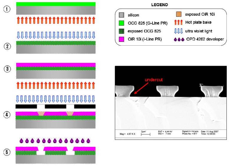
Figure 6 - LEFT: Bi layer lift off process parameters for
obtaining undercut features.
The method uses standard Microlab automated track spincoat and develop recipes.
RIGHT: Typical undercut profile
result for bi-layer lift off process.
- CMOS Baseline Extension for MEMS Testing
This past year I completed
and submitted the third layout of a MEMS electrostatic mono directional displacement
device for Microlab’s CMOS baseline. The latest MEMS structure contains a cantilever designed to rupture, presumably
at the test material’s rupture limit, and will complete the trio of variable
material MEMS testing devices for determining Young’s modulus, fatigue, and
rupture for a variety
of thin film materials. SiC, SiGe, and poly-Si are examples of the materials
that may be evaluated. Young’s modulus
and fatigue devices were designed and submitted for CMOS processing previously.
Note
that the fabrication steps of the MEMS structure are performed parallel to the
CMOS Baseline process flow, as depicted in Figure 7 and Figure 8. The post processing steps consist of a test-material
deposition, pattern, etch, and release (Figure
9).
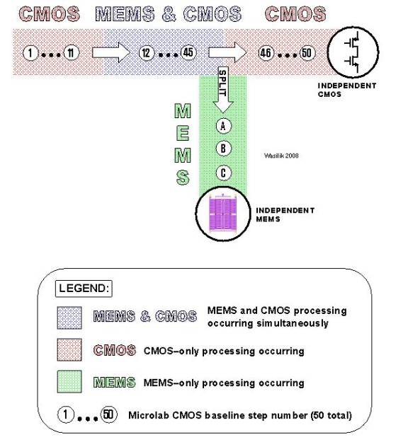
Figure 7 - Parallel
Processing with “Split” Schematic
Steps 1-50 to make CMOS,
MEMS “split” occurs after step 45.
Steps A, B and C then take
place to make MEMS devices.
Note: Final MEMS devices are standalone, not
integrated with CMOS.
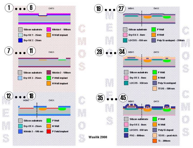
Figure 8 - Schematic of the 45
Processing Steps that Occur Before MEMS “Split”.
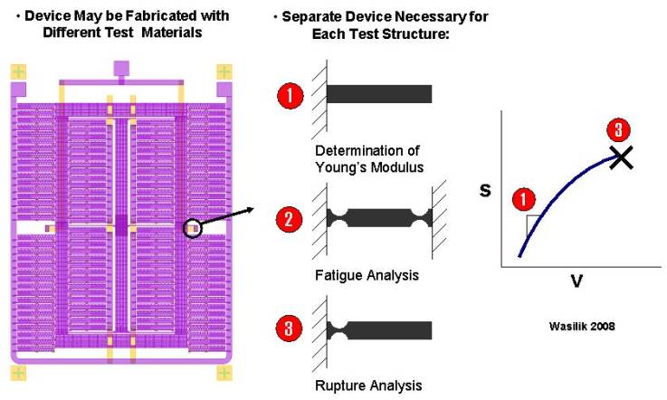
Figure 9 - Three
Different Types of Electrostatic Mono-Directional In-Plane Displacement
Microactuators
- Vapor
Pressure Spreadsheet
A
previously developed interactive gas vapor pressure spreadsheet (Figure 10) was updated during the
course of the year. Common etch gas vapor pressures vs. variable temperatures
are tabulated in the document, and posted online for Microlab staff use.
Applications of the spreadsheet are universal, but its original need stemmed
out of setting the proper mass flow controller pressure regulation at Centura
and other equipment. Anticipation and prevention of gas condensation in a
delivery line is the chart’s key function.
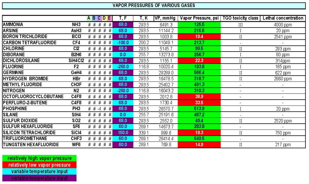
Figure 10 - Three Different Types of Electrostatic Mono-Directional
In-Plane Displacement Microactuators
IV.
OTHERS
- Probe Station Comparison Table
I evaluated and prepared a probe station comparison
table for BSAC Professor Nguyen. The table details differences and similarities
among several different commercial models. Cryogenic models as well as probe
heads are included in the tables.
- Textron Process Flow
I
worked to streamline, and develop a process flow outline proposal and bid
document for Textron Inc. (principal investigator: Professor Pisano). Some elements
of the process flow were deemed worthy enough to submit to UC Berkeley’s Office
of Technology Licensing.
- UC Davis Alcatel
I provided DRIE process consultation
for UC Davis BSAC with respect to their
lab’s Alcatel DRIE equipment over the course of the year. Current process
results were evaluated, and specific and generalized recommendations were
provided.
- Microlab Tours &
BSAC Luncheon Seminar
I served as default host for the
weekly BSAC lunch seminar. The following list is not inclusive, but I also provided Microlab tours for
the following companies/organizations: Toyota,
Kodak, NDK, Bridgewave, Vegrandis, and Brazil Aerospace.
V.
FUTURE GOALS
- CMOS Baseline
Extension for MEMS Testing
Fabrication and testing/verification of the electrostatic displacement microactuator that have been fabricated in the Microlab’s CMOS baseline process
will resume. A working device will have the capacity to test the mechanical
properties of different materials, including modulus of elasticity, fatigue,
and rupture. A known test material (such as polysilicon) will be processed with
the devices in 2008 to confirm functionality.
- Deep Reactive Ion Etch Monitor
DRIE etch monitoring for
both Centura DPS and STS will be reinstated in 2008. Wafers and SPC charts have
already been prepared. I will train and advise student lab assistants in
running the process monitor and tabulating the data.