MEMORANDUM
To: BSAC
Faculty Directors
William
Flounders, Microlab Technology Manager
From: Matthew
Wasilik, BSAC, Senior Development Engineer
Subject: 2008
Year-End Report
Date: 1
January 2009
cc: Katalin
Voros, Microlab Operations Manager
Professor Ming Wu, Microlab Faculty
Director
I have served as a development engineer for
the
I.
ENGINEERING, DESIGN, &
DEVELOPMENT OF NEW EQUIPMENT AND PROCESSES IN MICROLAB
· SUSS
PMC150 PROBE STATION
I evaluated and specified multiple potential site
locations in preparation for the newly acquired cryogenic probe station from
Suss Microtec. At least 5 different sites were considered. Autocad layouts of
the rooms, facility requirements, and equipment move logistics were presented
to Professor Nguyen and members of his group. Quick-glance table comparisons
were also submitted with final recommendations. I worked with The Cory Hall
Machine Shop concerning work request estimates as well as logistics of prep
work, receiving, transferring, and install of the probe station. The equipment
was successfully sited in 355 Cory. Post-install I helped to write and format
an operations manual that is to be posted online for upcoming users.
· PICOSUN ALD
I worked
to prepare and verify compatibility between the former RTCVD equipment load
lock and the newly incoming Picosun atomic layer deposition tool. Making use of
the RTCVD load lock mechanism ultimately provided a substantial cost savings
that would have otherwise been associated with the new ALD equipment.
· ALN
PIEZOELECTRIC ALUMINUM NITRIDE
The piezoelectric grade aluminum nitride sputter
equipment was upgraded to 6inch substrate compatible equipment this year. I
designed a silicon pocket wafer process flow for fabrication of a special wafer
carrier to provide continuation of 4 inch substrate processing at the tool. The
pocket wafer design allows wafer to rest on a silicon pocket eliminating the
need for adhesives. The process flow consisted of a dual mask exposure, with
front-back side alignment contact lithography. I worked to fabricate several of
these pocket wafers to meet the upgrade deadline. The carriers are currently
available for use with ALN.
· TYSTAR 15
I performed heat transfer analysis for verification
of a new water-cooled flange seal design augmentation at Tystar15. The
functional requirement for a silicone o-ring to withstand 1000 deg C furnace temperature
(methylsilane + H2 gas) was first established. I built a one-dimensional
conduction/convection model using Mathcad software, and thereafter determined
theoretical internal furnace convection coefficients. The results of the model
showed that the water cooled flange would cool the o-ring suitably. The flange
was installed at Tystar 15, and runs were made with success.
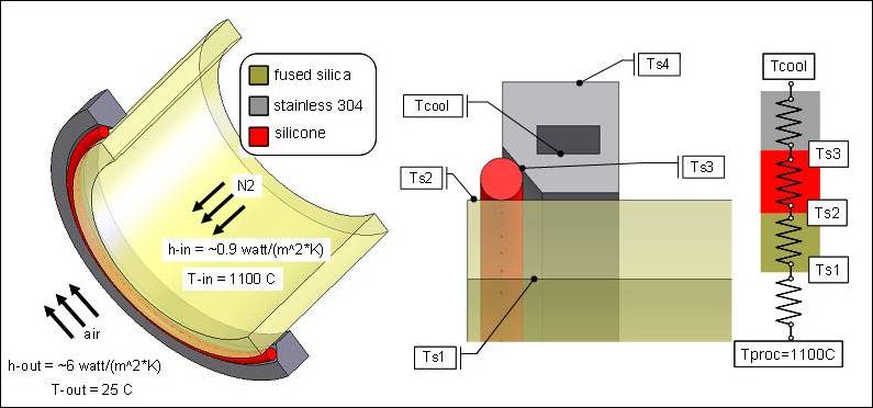
Figure 1
LEFT: Cross section of Tystar 15 furnace tube with
temperature conditions and coefficients.
RIGHT: Detail of surfaces analyzed and respective
thermal circuit model.
II.
SUSTAINING OF EXISTING TOOLSET &
SUPPLEMENTARY PROCESS DEVELOPMENT IN MICROLAB
· CENTURA DEEP SILICON ETCH
Much
effort and progress was made this past year with the 6 inch compatible DRIE chamber.
This equipment is expected to serve as “work horse” for 6 inch war DRIE
processing in the new Marvel Lab. Following observed process result anomalies
in late 2007, I performed work to systematically evaluate independent
components and sub systems as they related to process.
Gas Delivery
One
concern was that the C4F8 (Octofluorocyclobutane) gas was potentially
condensing to a liquid inside the delivery line. Because C4F8 has a low vapor pressure,
a condensed gas due to throttling though the mass flow controller was not
inconceivable. Cooling, and consequent condensation would hypothetically be
caused by a Joule-Thomson effect. Using a special generalized residual enthalpy
correction chart calculation, a temperature drop across the MFC was estimated.
The temp drop calculated from the model was ultimately too small to cause
condensation. In the course of this investigation, it was however noted that
the SF6 pressure was regulated much higher than the C4F8. A series of process
experiments showed that by lowering the SF6 regulated pressure substantial
improvement was achieved. Less black silicon notable. Thus the high partial
pressure of SF6 in a single gas delivery line may have contributed to small
amounts of C4F8 condensation.
RF Bias and Match Network
The
cathode bias was also extensively tested. I demonstrated that neither the
pulsing nor the low frequency (400 kHz) functions were working properly. The
matching network for the bias generator also became suspect. All of this
information was documented and presented to Applied Materials. Applied conceded
that the bias was not configured correctly, and what’s more the wrong type of
bias generator had been installed. A special HALO (high accuracy low output)
generator was put on order. Upon receiving the HALO, Applied service reps spent
several months troubleshooting and reconfiguring the generator to the system.
Both hardware and software were modified, and updated as necessary. I assisted
with process testing during this entire period, and furthermore provided
continuous recipe development for Labmembers that needed use of the tool. This
was performed concurrent with the aforementioned work. Eventually a proper
configuration was obtained. I worked to confirm proper pulsed bias operation,
duty cycle and period from the HALO generator. I am pleased to report all
reflected power issues with the matching network were verified as resolved.
A
historical summary of DPS equipment-use vs. encountered issues may be seen in FIGURE 2. Despite the various system
issues experienced throughout 2008 with this equipment, the DPS deep silicon
etcher was still capable of providing DRIE processing on 6 inch wafers for
those labmembers with patience.
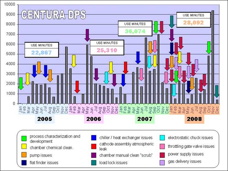
Figure 2 - Centura Use Chart vs. Problems Encountered (Updated for 2008)
Process Characterization
The
re-characterization of the DPS deep silicon etch process followed the
resolution of all outstanding mechanical and electrical system configuration
issues. A resolution V, 16-run factorial design of experiment was conceived and
performed. Five different factors were studied in this experiment: C4F8 and SF6
flows, C4F8 and SF6 pressures, and continuous wave (non-pulsed) bias power.
Once the data from the runs was analyzed, special fine-tune process runs were
performed to achieve results for application specific recipes. Results of a
newly developed recipe are contrasted with previous recipe performance in Figure 3. The recent
recharacterization of the chamber also served as a foundation for
implementation of routine statistical process control for the chamber. Etch
rate, uniformity, and selectivity monitoring commenced in November 2008. Detailed
monitor results are documented online for public viewing.
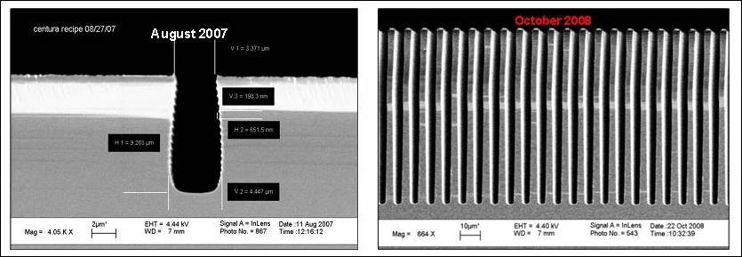
Figure 3
LEFT: DRIE results prior to mechanical and
electrical issues being resolved at Centura.
RIGHT: DRIE process results following recent
characterization.
·
FLIPCHIP BONDER
The Suss MicroTec FC-150 flipchip bonder is a high
performance bonding tool capable of performing thermocompression and solder
reflow processing. I continued to serve as an equipment and process support
engineer on this equipment in 2008. I troubleshot issues as they arose, and
made recommendations to Microlab technical staff and third party vendors when
necessary. Regimented operations training, instated formerly, has continued to
succeed in preventing user errors with the tool. I continuously provided process
consultation on this tool. Although not without issues, for the better part of
the year, flipchip performed well for most applications.
SET (Smart Equipment Technology;
Flipchip encountered a serious stage crash in
August that eventually required third party vendor service visit. Equipment
software parameters needed resetting due to the crash. Several days following
this fix the Zerodur thermode thermocouple detached from the arm. Microlab
technical staff was able to skillfully repair the thermocouple in-house, not an
easy task. Unfortunately more independent problems followed: PC power supply
failure, corrupted DI/O PCB card, temp sensor wiring, large misplacement from
faulty N2 chip blowoff circuit, and more erroneous software equipment
parameters. Through perseverance, staff worked in team effort to solve all
these problems.
A cost / benefit analysis evaluation for flipchip
may be seen in FIGURE 4. This past
year produced the highest recharge for the tool yet. The study projects a
recoup of cumulative equipment costs (Y2005-2008) in 2009. A larger researcher
base is anticipated as reliability continues to be improved. I consider
flipchip a case example that establishes when properly managed, even the most
sophisticated systems are sustainable in an all-inclusive research environment.
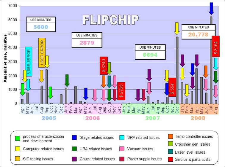
Figure 4 - Cost-Benefit Study for FLIPCHIP
·
STS
STS
continued to perform exceptionally as a deep silicon etch tool for Microlab and
its labmembers in 2008. The equipment accumulated 8000 minutes of use per
month on average this past year. I continued to support operation and
processing aspects of this important machine.
Process
I continued my efforts at educating labmembers on
the specifics of DRIE processing as needed. Aside from the routine training and qualifications on the
tool, I provided process support for researchers and staff members alike. Because
process drift with DRIE is inevitable, I served to develop and fine-tune recipes for specific
applications upon request. The main cause of process drift at STS is
thought to be carbon-rich byproduct accumulation on the chamber walls over time
(sputtered resist, passivation gas deposits, etc.). This buildup changes the
plasma chemistry, and results in a net reduced fluorine availability. Process
drift at STS occurs in cycles. Typically, Microlab’s STS chamber experiences 3
etch regimes over a six month period. The first stage follows a clean ceramics
install, and is characterized by aggressive, reentrant profile etches. A
moderately used chamber defines the second stage, most recipes in STS database
were developed for this regime. The third and final stage of the chamber is
distinguished by lessened etch rates and etch “energy”. This is due to lessened
available reactant, but recipes may still be adjusted to produce similar
results as previous. At the end of the third stage, cleaned ceramics are
installed, and the cycle begins again. The statistical process monitor instated
at STS this past year produced data that supports the theory outlined above.
Such data is presented in Figure 5.
Etch rate,
uniformity, and selectivity is now monitored at STS on a routine basis by
Microlab student workers. The information is documented and presented online
for public viewing.
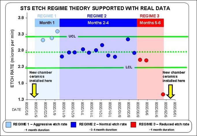
Figure
5 - Etch Regime Theory Superimposed With
Real Etch Rate Data
Acquired From STS Routine Statistical
Monitor
I also
created a quick-glance process trends chart based on first order STS process
performance trends for submission to Microlab process staff. Information
contained within the chart provides concise instruction for adjusting recipe
parameters, with case examples, and presents the distinct process cycles that
the chamber experiences over a period of 6 months. In my absence the chart may
be used to fine-tune recipes as needed, something I am often asked to do.
Mechanical and Electrical Issues
I worked with STS personnel to troubleshoot and ultimately replace the
physical capacitor assembly in the coil match network. The old capacitor
assembly was shorting and causing coil tolerance errors during processing.
Subsequently, I worked to address an unexpected RF interlock display unit
failure. A new module was specified, purchased, and installed. The turbo
molecular pump and controller also failed in 2008, and I performed an
evaluation of different turbo pump configurations for DRIE processing.
Molecular drag stage, foreline pressure capacity, throughput, and by-product
build-up resistance pumps as compatible replacements were reviewed and
tabulated. This Information was consolidated into a color coded table format
and presented to lab management. Ultimately a Seiko Seiki STP1301 turbo was
successfully installed. Having the Seiko Seiki turbo at STS facilitates
maintenance, as most major etch tools in Microlab use this type of pump.
Shortly thereafter, a chamber vacuum leak was encountered, a fourth consecutive
yet independent problem at the machine. I persevered to troubleshoot and eventually
found the leak to be in an auxiliary valve on the chamber port. The valve was
replaced with success. An additional gas interlock was added to the STS this
past year after problems became relevant with labmembers attempting to bypass
recharge with the tool.
6-Inch Upgrade
The 6-inch upgrade of STS was to take place in
2008, but was inevitably delayed. A commitment to have a reliable pulsed-bias
process working at Centura-DPS before upgrading STS to 6-inch was made. Delays
at Centura, as well as prolonged issues at STS caused the upgrade to be pushed
back. All parts for the STS upgrade were acquired, and this is slated to take
place in early 2009..
· CRESTEC
I underwent training on the new Crestec e-beam lithography
system with the intention of providing process
assistance for BSAC researchers on this equipment. The system has demonstrated
capacity to write 10nm resolution features. I specified and ordered
phosphor-bronze clamps for holding dies, an improvement from “taping” small
samples to the chuck. I also had the opportunity to troubleshoot and solve a
minor issue with the equipment while several Microlab technical staff were on
scheduled leave. This kept the machine up and available for processing.
III.
PROJECTS
· LIFTOFF PROCESS CHARACTERIZATION
I
investigated multiple standard and non-standard lift-off methods previously.
This project’s main goal was to study, verify, and define a baseline lift-off
process for use by a large group of researchers with a broad range of
conditions. A bi-layer process was ultimately selected as a preferred means of
performing liftoff. This preferred method uses standard stock resists, and no
special chemicals are required. The preferred bi-layer method also uses
standard recipes on the spincoat tracks, thus facilitating processing.
Following the online documenting of this process flow, labmembers began to
register complaints that the bi-layer method had flaws. One claim in particular
was that the flood exposure was not necessary and even detrimental to the
liftoff profile. Rather than let rumor and superstition rule the lab
environment, I addressed such by performing a follow-up Box-Behnken response
surface study in the attempt of providing elucidation on these claims. The
design of experiment consisted of 15 runs. Flood exposure intensity, critical
exposure intensity, and develop time were investigated at three different
levels respectively. The results of the experiment gave insight, perhaps even
more than originally anticipated. It was found that a flood exposure contributed
largely to decreasing variability in liftoff profiles. Thus, the experiment
predicted that those labmembers skipping the flood exposure step would
invariably not be happy with the results. The original process publication was
authenticated, in that a proper flood exposure was an important step in the
process. All of this information was
documented for online viewing and furthermore reported at the bi-annual BSAC
industrial advisory board meeting.
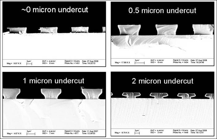
Figure 6 - Demonstration of the
Pictures show photoresist profile on silicon.
Insight taken from the Box-Behnken response surface design performed.
· CMOS BASELINE EXTENSION FOR MEMS PROCESSING
This project involves the fabrication of a MEMS
electrostatic mono directional displacement device by using Microlab’s CMOS
baseline. The project was unfortunately placed on the back burner for much of
2008 due to other high priority issues in the lab. I am pleased to report
however that a final mask set for the devices that measure Young’s modulus was
designed and completed. The steps remaining to prove functionality of the
device involve depositing a test material, in this case poly silicon, then patterning
and releasing the device. Future structures, already made with the CMOS
baseline process, will have the capacity to measure fatigue and rupture
strength. Note the structures do not have to be made of poly silicon, such is
for verification purposes only.
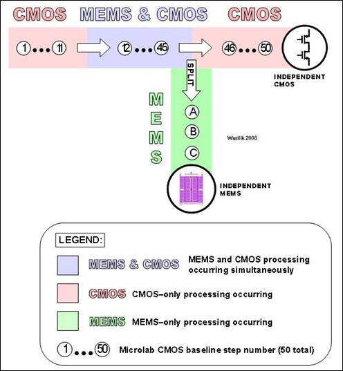
Figure 7 - Parallel Processing With “
Steps
1-50 to make CMOS, MEMS “split” occurs after step 45.
Steps
A, B and C then take place to make MEMS devices.
Note
final MEMS devices are standalone, not integrated with CMOS.
IV.
OTHERS
· BSAC
INDUSTRIAL MEMBER VISIT
I co-hosted BSAC members Starkey for one full day
in August 2008. A presentation on Microlab process capabilities, discussion,
and detailed lab tour was provided.
· GRAPHICAL
DISPLAY OF INFORMATION
I worked
to improve my skills with graphical display of information. Examples are
included in this report.
· MARVEL LAB CAD LAYOUTS
Being a
staff member proficient with AutoCAD, I organized and formatted multiple
AutoCAD drawing layouts of the new Marvel Lab for plotting and reference.
· MICROLAB
TOURS & BSAC LUNCHEON SEMINARS
I served as default host for the weekly BSAC lunch seminar. I
also provided Microlab tours for current and potential BSAC industrial
members as necessary.
· PROCESS CONSULTATION
I assisted BSAC labmembers with process questions
regarding DRIE, various plasma etch, various wet etch, molecular vapor
deposition, HF vapor release, SEM instruction, wafer bonding, mechanical and
optical profiling, IR camera microscope inspection, thermocompression bonding,
contact lithography, flipchip bonding, and liftoff during the course of the
year.
V.
FUTURE GOALS
· CMOS BASELINE EXTENSION FOR MEMS
PROCESSING
I will complete the fabrication and
testing/verification of the electrostatic displacement microactuator that was
fabricated in the Microlab’s CMOS baseline process. A working device will have
the capacity to test Young’s modulus of different materials. A known test
material (such as polysilicon) will be processed with the devices to confirm
functionality.
· MARVEL LAB
MOVE
I will be heavily involved with the move to the new
lab. During the past year I have worked to successfully instate process
monitoring on “high profile” equipments. Such will serve as a baseline for
process start up for these machines when in the new lab. Further detailed
baseline tests on equipments under my responsibility will also be required
before their move. I will furthermore perform mechanical/electrical design with
respect to the move as necessary.
· PICOSUN
I will perform a design of experiment
characterization for this new equipment, and create a baseline test prior to
its move into the new lab.
· SUSS
PMC150 PROBE STATION
I will continue to actively support this
BSAC-specific important equipment.