MEMORANDUM
To: Katalin
Voros, Operations Manager
From: Sia Parsa,
Process Engineering Manager
Date: 23 January 2009
This
memorandum documents process engineering activities for the calendar year 2008.
Last year, I supervised the process engineering group comprised of 4 process
engineers, including; one MEMS-Exchange engineer, as well as the baseline
research associate, and average of three lab assistants (undergraduate
students) and one graduate student researcher in the Microlab.
It was a
very productive year both in terms of maintaining the operation and generating
record amount of revenue through staff service/support of BMLA members and
other universities. These activities along with installation and
characterization of new tools in the Microlab kept staff challenged and very
busy throughout the year. There were total of 10 training sessions (2 days
each) offered by staff on the new Crestec E-beam writer machine. The Picosun
ALD machine, our other new tool in the lab required direct staff involvement
during the acceptance and process development phase. SVG coater 1, 2 and 3
tracks were also converted to increase our six-inch capability, while still
offering four-inch processing in the Microlab. A complete rebuild of the
six-inch developer track greatly improved mechanical performance of the tool,
also increased its memory storage to save up to 99 recipes (old version could
only save up 9 recipes).
Last year,
the last and final version of the MEMS-Exchange runs under the Plastically
Self-Aligned Micro-Mirrors project was completed. This run yielded much
better than the previous runs, partly because of the suggestions made by staff
at the conclusion of the second run (R3506), as well as cumulative knowledge
gained through the design and processing of previous runs.
Process staff was involved in many other tasks including
preparation for the new lab. The following summarizes Process Engineering
activities for 2008 (last) year.
II.
EQUIPMENT UPGRADE & NEW INSTALLATIONS
Crestec e-beam Lithography
System (New)
Last year, a High Resolution Electron Beam Lithography System was
installed in 197 Cory Hall. The new
Crestec e-beam writer, model CABL-9000, successfully passed the qualification
test in February (10nm isolated features and <20nm stitching accuracy over a
50 micron square field). The inspection
of tool by equipment staff at the vendor site and receiving basic training on
the tool helped the smooth transition of the tool into our lab. The Crestec
engineers were also very helpful and courteous, quickly offered the first round
of training to our designated staff, Kim Chan, and selected members. Kim then
promptly held the first training session for other members in late February,
and since then a total of ten 2 -day trainings have been completed. This
enabled around 30 qualified members on this rather sophisticated tool in the
Microlab. The Crestec manual is now at
its third revision, with base processes listed for different types of PMM
resist (different molecular weight). PMMA resist is a great alternative to a
much more expensive and exotic resist/s recommended and used by Crestec
(ZEP-520A positive resist from ZEON Chemicals or negative tone
inorganic Hydrogen silsesquioxane (HSQ) are much more costly and are not needed
for most of our applications).
Picosun ALD System
A new Picosun Atomic Layer
Deposition (ALD) system, made available through a grant by Professor Clark
Nguyen was quickly installed and qualified in the month of November. The new system comprises of a wafer loader
station, a deposition chamber, a
source cabinet with associated electronics and MFCs, all of which are
controlled by the Picosun software installed on a PC that is connected to a
user-friendly touch control panel. I worked closely with the field engineer at
the initial stages of the installation and acceptance of the tool. The tool
passed the acceptance test in November (490Aº thick film deposited at less than
three percent non-uniformity). Jimmy was assigned the task of receiving
additional training and qualifying members on the tool. There are currently two
metal sources available on this ALD machine.
Trimethylaluminum Al (CH3)3 is the source used for depositing aluminum
oxide and Tetrakis Isopropoxide (TTIP) used for Titanium oxide deposition. The
titanium oxide process is a somewhat slower process; 1/4 of the deposition rate
as compared to the aluminum oxide currently at 1Aº/cycle deposition rate. The
task of qualifying and process development has required close collaboration
between staff and Microlab members who seek their special application processes
on this tool. Jaeseok Jeon and Vincent Pott investigated electrical quality of
200Aº thick aluminum oxide film deposited on P-type substrates. Chemical
resistance and MOS capacitance performance of aluminum oxide dielectric was
measured (P-substrate/Al2O3/AL stack), results were as per follows:
-
No
significant film thickness loss in HF vapor (up to 21 minutes exposure was
attempted).
-
Significant
film loss in 5 minutes of BOE/piranha (~18.6 nm out of 20 nm original film
lost).
-
No
significant change of the film thickness after applying 5 minutes of RTA in N2
ambient.
SCA measurement of the film after the RTA:
Nsc = 4.70E14
Qox = -1.97E12
Dit = 3.37E11
Qfb = -1.78E12
Ts = 45
n = 1.7
-
The I-V curve of NMOS capacitor
structures with different dielectric thicknesses were also measured on various
sites on the wafer for 0 to 2volts bias condition. Following data is from the
center location:
A. NMOS capacitor (300 nm Aluminum/20nm aluminum oxide/p-type
substrate)
Maximum leakage current at 2 volt bias = 28.35 nA/cm2
Minimum leakage current at 0 volt bias = 2.1 nA/cm2
B. NMOS capacitor (300 nm Aluminum/3nm aluminum oxide/p-type
substrate) :
Maximum leakage current at 2 volt bias = 204 nA/cm2
Minimum leakage current at 0 volt bias = 0.13 nA/cm2
Shallow Junction Diffusion Process
There was a need for a very shallow p-type junction requested for
the MEMS-Exchange run R4521. I was able to have the customer at MEMS-Exchange
pay for the SRP work that was needed to target their desired shallow junction
depth (relative to our standard process). They originally asked for 1um, but
later opted to go with XJ ~1.9 µm. Diffusion process was performed
with three groups of wafers at three different process times in Tystar14,
14SB+O2 recipe at 1050ºC. Drive in was
fixed in Tystar3 at 900ºC for 30 minutes followed by 5:1 BHF for 15 minutes to
strip the top oxide. This was a valuable free of charge analysis, yielding
interesting results at 0.5, 1 and 2 hrs diffusion times that had not been
characterized earlier. We had always
aimed at MEMS applications and deep junction depth in the past. This was a
useful additional data point that complemented our old data set generated a few
years back.
Junction
depth at three diffusion times
0.5 hr
diffusion process: XJ= ~
0.88
1 hr
diffusion process: XJ=
~1.6 µm
2 hrs
diffusion process: XJ
=1.9 µm
Six-inch SVG Developer Upgrade
After many years of patiently waiting for the SVG developer
upgrade to eliminate the leaky stationary nozzles at this station, the
opportunity arose in the summer at a reasonable price tag. The process group
went out of their way to accommodate the change. I worked through weekend of
September 13th to make sure the tool would have minimum downtime
during its upgrade. A basic DUV develop process was then made available that
Saturday. Other developer recipes were soon released for I-line and G-line
resists, as well. The retractable arm has made the tool much more reliable and
trouble free.
III.
PROCESS
DEVELOPMENt, sustaining &
IMPROVEMENT ACTIVITIES
New Processes
-
New processes were released on all of
our new equipment installations (Crestec e-beam lithography, Picosun ALD and
six-inch SVG coat and develop machines).
-
Low stress silicon carbide process was
tested by Daniel Queen in Tystar15. This process uses DCS, DSB and NH3 gases
with a deposition rate of around 53 nm/min. A full report is available at the
Microlab web site, following link:
http://microlab.berkeley.edu/text/processreports/SiC.pdf
-
Hot Aluminum process was tested by our high
school summer intern, further refined by Daniel Queen, a Two-Step Hot
Aluminum (TSP) process in the Novellus m2i machine. A high temperature
treatment (500ºC) is used to reflow an aluminum film that has been deposited at
low temperature (300ºC). This process improves the metal step coverage inside
the contact and via holes, enabling more advanced technologies. Please note;
the initial temperature of the wafer is critical for good reflow of the
deposited aluminum film. To ensure that the wafer is at a suitably low
temperature, the Ti adhesion layer station needs to completely cool (~12 hrs
from 300°C to 50°C) prior to starting deposition. The SEM pictures of 2 µm
contact holes in Figure 1 show much better contact coverage by the hot aluminum
process (Figure 1b), as compared to the standard aluminum sputter process
(Figure 1a).
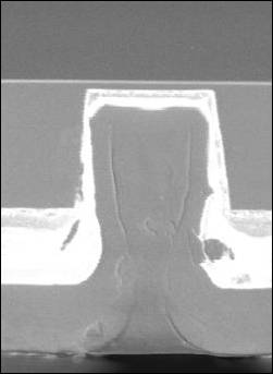
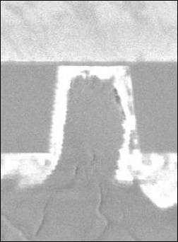
Figure 1 - Cross Sectional SEM of a 2 µm Wide and 2 µm Deep
Contacts
(a)
Cold Aluminum Poor Step Coverage
(b)
Hot Aluminum Process Improved Step Coverage
Current Processes
-
Due to a long lead time associated with
DUV resist manufacturing/delivery, resist usage was closely monitored by
process staff to ensure no shortage of resist would occur. BARC and other
support material were also monitored and ordered by the process staff in a
timely manner. Process group also
investigated a BARC batch problem by contacting vendor and running experiments
on the track (different bake time/temperature and delay time).
-
A set of parylene experiments were
conducted by Attila for our BSAC engineer (Matt). A linear relationship between
the thickness of deposited parylene and the amount of dimmer used to deposit
such film was established.
Parylene-C
thickness (µm) = 1.339 X amount of C dimmer mass (g)
Parylene-N
thickness (µm) = 0.4086 X amount of N dimmer used (g)
Equipment Support
Wafers Saw
-
Daniel Queen, our graduate student
researcher, experimented with six different types of blades (various
length/width) aimed at selecting one possible solution to all our silicon
dicing needs, including double bonded six-inch wafers (the thickest possible
stack used in the Microlab). I provided Daniel with different type of blades
and some bonded oxide wafers that had been prepared earlier. He quickly settled
on the Keteca K3T20L45 blade. The wafersaw manual was updated with the
following specifications:
Keteca,
P/N K3T20L45 blade specification:
kerf (width of cut) = .45 microns or .0018”
Maximum depth of cut = 1.140 mm or .045”
Maximum
Cutting Speed: 3 mm/se
ASML
-
The ASML reticle stage was severely
damaged by the poor quality of an incoming reticle that was purchased from an
outside vendor and used by one of our Microlab members. The original cost of
the repair estimated at $122,571.33 was negotiated down to $90,811.73 (including
tax) through 35% exchange credit and an additional discount that was approved
by ASML management. I worked very closely with the ASML to negotiate the cost
and expedite the repair. ASML Company took about a month to make the
replacement parts available to us, and more than a week to install it on our
tool. Rosemary vigorously pursued the financing part of the deal and was able
to get the campus Risk Management office involved with a third party assessor
assigned to our case. Evan and I worked closely with the assessor, provided him
with necessary information, access to the tool and digital pictures for the
appraisal. I am delighted to report that
we were able to recover most of the repair cost ($85,317) through campus
insurance. Great collaboration between
all parties involved, getting us back to normal in a relatively expeditious
manner, and considering the enormity of the damage involved. Bob and the
machine shop (Ben) later provided us with a nice fixture (reticle template)
that can be used to check quickly and accurately the size and shape of an
incoming reticle. I updated the ASML manual for all qualified members to
inspect their incoming reticles on this fixture, so that there will be no
chance of such a mistake ever happening again!
Xetch
-
The equipment engineer in charge of the
Xetch, Joe requested that we set him up with a quick method of checking the
health of the XeF2 machine (Xetch), after repair or in case of a problem
report. I proposed that we pattern and
etch 10 oxide wafers with different size structures to baseline the Xetch etch.
The following steps were taken to generate the test chips needed for the Xetch
monitoring:
-
Laszlo designed a die with lines/spaces
of various size/density for this test mask.
-
Kim patterned (ASML) and etched
(Centura MxP+) eight oxide wafers (280 nm oxide).
-
Wafers were then partially diced, so
that the test chips can easily be snapped off.
-
Resist was then removed from these
wafers so that the patterned oxide can be used as a hard mask for silicon
etching and the ASIQ machine to determine etch depth/rate.
Tylan17
(LPCVD LSN Process)
-
Excellent troubleshooting was performed
by equipment (Danny) and process (Jimmy) staff on a major process pressure
issue reported on Tystar17, early October.
Many steps were taken to narrow down the root cause of the failure,
including process check at different stages of the repair that ultimately
brought the tool back on line. The rear of the tube was severely choked up by
hardened material; therefore, the tube had to be replaced. Process ultimately
checked out and the tool released to Microlab members.
Lab Manual Write-Up, Process Monitoring, and Qualification Tests
Last year,
process, BSAC, and Baseline engineers updated all the lab manual chapters
assigned to them with revision dates older than 3 years (listed below).
Microlab equipment engineers and technology manager, as well as selected number
of Microlab members took part in this overall effort to keep our lab manuals up
to date.
New and
Rewritten Chapters
Chapter 1.3 - New MOD 37 - Processing
bottom Anti-reflective coating (10/08).
Chapter 3.3 - Complete rewrite of GCA
pattern generator chapter to the new format (08/08).
Chapter 4.24 - Total rewrite for a
standalone SVGCOAT6 chapter (09/08).
Chapter 4.26 - Rewrite of the SVGDEV6 chapter post hardware
upgrade (11/08).
Updated
Chapters
Chapter 1.2 - Added a note in chemistry
safety section of the Microlab safety rules (11/08).
Chapter 1.5 - CMOS process flows posted
for 6" substrates (2008).
Chapter 1.6 - Edited wafer substrates
chapter (08/08).
Chapter 1.8 - Updated equipment list on
4" &6" tool compatibility chapter (05/08).
Chapter 2.2 - Minor changes made to
Tystar and Lam rework chapter (07/08).
Chapter 2.3 - N2 flow-meter procedure
added to Sink3 chapter (09/08).
Chapter 2.4 - Hot plate safety notes
added to sinK4 chapter (11/08).
Chapter 2.5 - Updated the sink5 chapter
with current information, no HMDS bubbler (08/08).
Chapter 2.6 - Removed obsolete
references, expanded on sink6 protocol section (09/08).
Chapter 2.9 - Changed the purpose and
processes allowed in sink9 (09/08).
Chapter 2.11 - Added bases to the list of
chemicals that can be aspirated in sink432A (09/08).
Chapter 2.14 - Updated Tousimis CPD chapter with schematics of the plumbing (10/08).
Chapter 3.1 - Updated plotter
info/command lines in sections 2.4.1 in
CAD chapter (03/08).
Chapter 3.2 - Reviewed and made minor
changes to GCAWS2 chapter (03/08).
Chapter 3.8 - Few additions and updated
CMOS Baseline Test Chip chapter (03/08).
Chapter 4.0 - Minor editing of the
general resist parameter chapter (04/08).
Chapter 4.11 - Added
procedure for inspection of incoming reticles to ASML chapter (04/08).
Chapter 4.13 - Clarification
of the operation throughout the GCAWS2 chapter (07/08).
Chapter 4.16 - Modified
Subsections 9.9.1 and 9.9.2 of Quintel Mask Aligner chapter (07/08).
Chapter 4.17 - Added 10.2.2.15 & modified 10.3.1-10.3.6 in JEOL 6400 chapter (10/08).
Chapter 4.18 - Removed mark-ups and added
them in the content of Crestec chapter (11/08).
Chapter 4.21 - Separated and revised the
SVGCOAT1 chapter post 6” conversion (08/08).
Chapter 4.22 - Separated the SVGCOAT2
chapter, which has stayed 4-inch (08/08).
Chapter 4.23 - Revised the SVGCOAT3 coater
chapter post 4” conversion (08/08).
Chapter 4.28 - Modified section 9.1 of the
Matrix 106 with additional information (12/08).
Chapter 4.30 - Added safety sentences about
the hot plate in Spinner1 chapter (11/08).
Chapter 5.1 - Edited subsections 8.1.1,
8.1.2 and 9.5.11 of the Tystar1 chapter (03/08).
Chapter 5.9 - Deleted references to
section 9.2.7 and 9hstnbya recipe in Tystar9 (03/08)
Chapter 5.11 - Renumbered Section 5.10 and Inserted new Section 9.2.3 for Tystar11 03/08).
Chapter 5.20 - Minor changes made to
Tystar20 chapter (07/08).
Chapter 5.30 - Updated gas sources and
oxidation recipes used in the MOS furnaces (10/08)
Chapter 5.31 - Changed all references to
Heatpulse 2, also added pictures (03/08).
Chapter 6.02 - Revised section 8.1.2 and
10.4 and fault recovery in Novellus chapter (04/08).
Chapter 6.03 - Deleted Pt target no longer
available for the Randex machine (01/08).
Chapter 6.04 - Updated the CPA chapter with
clarification of operating instruction (07/08).
Chapter 6.07 - Define power density for
ITO, dielectric (W/cm2) in Edwards manual (12/08).
Chapter 6.08 - Deleted 6.3,
modified 8.4 materials restrictions in AMS manual (05/08).
Chapter 6.12 - Added section 10.1 about
vacuum system luck-up in Veeco 401 (03/08).
Chapter 6.14 - Added notes in subsections
5.08 and 9.17 of Edwards EB3 manual
(09/08).
Chapter 6.23 - Minor change made to the
AMST Molecular Vapor Deposition manual (12/08).
Chapter 6.29 - Minor change made to Oxford2 manual (07/08).
Chapter 6.30 - Updated PQECR manual to include
silicon nitride, a-Si process (12/08).
Chapter 7.0 - Updated lam etcher
overview chapter with minor changes (07/08).
Chapter 7.6 - Added subsection 9.3.5 in
Centura MxP+ (06/08).
Chapter 7.8 - Updated STS manual with
location of turbo controller (09/08).
Chapter 7.13 - Reviewed and added anecdotal
information to XeF2 manual (04/08).
Chapter 7.15 - Added section 8 to HF vapor
manual (11/08).
Chapter 8.04 - General probe station
chapter was reviewed and checked out (05/08).
Chapter 8.11 - Extended the Alpha step
specification and added surface roughness (10/08).
Chapter 8.13 - Minor changes made to Wyko
chapter (05/08).
Chapter 8.21 - Minor changes made to
Reichert chapter (08/08).
Chapter 8.32 - Troubleshooting guidelines
added to Sopra manual (03/08).
Chapter 8.44 - Updated section 6.2 of the
X-Ray diffraction machine (09/08).
Chapter 8.54 - Updated file transfer
procedure on contact angle machine (09/08).
Chapter 9.00 - Added KS-Aligner table to
Bonding tools overview chapter (06/08).
Chapter 9.4 - Formatted the Westbond
wirebonder chapter(03/08).
Chapter 9.6 - Clarification on operating
procedure for the dicing saw chapter (07/08).
Chapter 10.1 - Clarification on operating procedure in the CMP chapter (07/08).
New Process Reports link
I initiated a
link for process related reports, which could eventually centralize process
reports/information for general use. This way process related development
work/reports are immediately visible in the process panel of the Microlab web
site.
Process Monitoring,
Equipment Training, Member Qualification, and Test Grading
Last year o
A large
number of equipment qualification was performed this past year, written test
(graded), and oral tests were given by staff for number of tools. The BSAC and
baseline engineers also provided support in the DRIE etch, metrology, and CAD
layout/ mask making areas. I assigned superusers on various tools and helped
administration staff reinstate some of our members on their expired equipment
qualification.
New lab
Support
Process
staff provided all the requested information to Dr. William Flounders, our
Technology Manager to plan ahead for the new Marvell lab. We submitted an excel
sheet outlining our current storage
inventory, sink layouts for the new lab, as well facility requirements for each
equipment migrating to the new lab. The
facility requirements for each tool on the list was generated by the equipment
engineer in charge of a particular tool, and compiled by Attila.
IV.
process Staff Supervision,
TRAINING & OTHER SERVICES
Staff Supervision: I Continued my supervision of process/MEMS-Exchange engineers, one
baseline assistant specialist, as well as one graduate student researcher (GSR
25%), and three undergraduate assistants working in the process group. Process
staff yearly appraisals were submitted on time, before the September 1st
deadline. Last year, I also mapped all
of our job titles to new categories defined by the university.
Promotion and Awards: Last year Kim received her 30 years service award for many
years of consistent and reliable service in the Microlab. Chris Zhao also
received the SPOT award. Chris has provided excellent and beyond the call of duty
service during his 2 years of working as a lab assistant in the Microlab. He is
starting the graduate school this year and will continue working in the
Microlab as a Graduate Student Researcher.
High School interns: Microlab was able to
continue our 6 year old summer internship program with two new high school
students; Kelsey Brokaw and Alice Wong. Jimmy Chang (senior process engineer)
and Daniel Queen (PhD candidate) provided mentorship and helped the interns
conduct process optimization work in the Microlab. The results of their
experiments were presented to the Microlab staff and guests at the conclusion
of their summer internship, as follows:
-
Kelsey Brokaw conducted her work in the
CMP arena. The effect of different process parameters on the oxide polishing
rate and removal uniformity were examined. She determined that both down
force and backside pressure had significant impact on etch rate and
percentage of the film non-uniformity; she developed an optimized recipe that
had high back pressure and down force. Kelsey also concluded that we could
perhaps extend the life of our polishing pads, as the old pads still had some
life in the them.
-
Alice Wong compared the hot and cold aluminum
processes in the Novellus m2i system. This project gave her the opportunity to
use various equipment including sinks,
furnaces to grow an oxide layer that was then patterned and etched (ASML)/Centura MxP+) to create via holes for her experiment. She
concluded that the two step hot aluminum process provides better via step
coverage than the standard sputter aluminum process. Addition of 500Aº Ti
underlayer as an adhesion (glue) layer further enhanced step coverage by
capillary action that helped draw down
the aluminum inside the via holes.
Microlab, EE143: Process staff
continued their service/support of the EE143 lab by ordering new furnace boats,
and supplying the class with their chemical needs, and helping TAs with their
poly/oxide runs.
Member advising, Help/Support of Other Universities, Institutions
-
Helped a colleague from University of
Arkansas with her MOS and non-MOS cleaning protocol questions, Input
gases for a PECVD process and percentage of SiH4 in Argon was also recommended
along with a basic recipe for her PECVD oxide process.
-
Helped colleagues and graduate students
at Stanford with their process/equipment questions; discontinuation of LDD26W
develop both here and at Stanford prompted common interest. Their question
regarding a viable Cr etch was promptly answered with available etch rate data
and a Cl2 + O2 based recipe. There was also an interest in the recipes
currently used for aluminum nitride etching at our site. The information
regarding the lam3 AlN etch recipe with double the amount of Cl2 and turning
off the N2 in the main etch step was forwarded as a good starting point to
develop their AlN etch recipe. SCA and
CV plot questions were also answered by sharing our method of pass/fail
criteria and the upgrade performed earlier, as a recommendation for their tool.
-
Held weekly meetings with process
staff, discussing Microlab issues.
-
We helped Michael Helmbrecht with his
G-line exposure feasibility question on our six-inch I-line stepper (GCAWS6).
Marilyn ran G-line resist coated wafers through this stepper and was able to
resolve 0.7 µm G-line resist lines at
1.0 second exposure time. This was good news for us too, as we can basically
phase out our 4” GCAWS2 stepper, when we move to our new six-inch Marvell lab.
I also helped Michael develop a Mix&Match process between GAWS6 and the
ASML stepper that addressed his non standard die size, and required a few
tricks to get the target positions right (global alignment step on theGCAWS6).
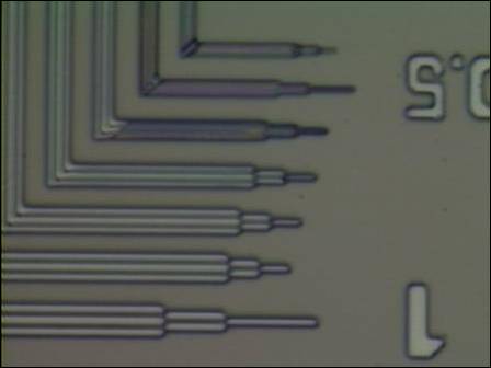
Figure 2 - 0.7 µm G-Line Resist Fork Patterns
Exposed on GCAWAS6 Stepper
V.
Semiconductor Processing &
special Services
ETR Services
Last year process staff completed 17 engineering test
requests generating $33,651.97 in revenue for the Microlab. In addition to the standard
processing normally offered in the litho, etch and the diffusion areas, we
performed other types of non-baseline processes for various universities, which
included;
MEMS-EXCHANGE PROCESS service
Last year we continued our services/support of the
MEMS-Exchange program with one local MEMS-Exchange (MX) engineer assigned to
the task of processing MX runs in the Microlab. These runs generated $18,269.10
in revenue for the Microlab. Attila Szabo, our MEMS-Exchange engineer
successfully completed the third and final version of Professor Lewei Lin’s MX
run in November (R4119). This run incorporated design/process improvement ideas
accumulated by the fabrication of previous two runs in the Plastically
Self-Aligned Micro-Mirrors project also utilized staff recommendation
outlined in my last 2007 annual report. Following modification were made to the
new run:
- Added more test
wafers to optimize all of our critical DRIE process steps, before
committing the product wafers.
- Added backside
polysilicon strip step (16) to the new run. We had oxide/poly/oxide
stack going into the last steps of the process in the previous run, which
somewhat complicated/compromised the backside etch process.
- The polysilicon
filled trenches on the front side were oxidized (step17) to prevent
polysilicon loss during later device etch steps (26).
- Changed the active
design area for better wafer mounting (wafers were mounted with their
device side down for the backside etch step). The test chip’s overall
dimensions however was kept the same, which enabled us to use the same HF
vapor clamp as was used for the previous run (Figure 3). Note: R3506 provided adequate scribe
line width in the vertical direction (Y), only.
- Increased oxide
layer for the backside etch.
- Improved (PR bake)
for backside DRIE mask.
- Instead of
cool-grease in R3506 run, we used laser-cut thermal release (Figure -3) to
mount product wafers on the carrier wafers in the latest run, R4119. This
eliminated the cool-grease contamination issues observed on the previous
run; however, presented delamination problems during the backside etch
step. Product wafers had to be remounted several times to finish this etch
step in the process.
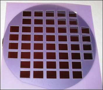
Figure 3 - HF Vapor Clamp (left) and
Thermal Tape Laser Cut To Correct Die Dimension (right)
- Changed the design rule
for the backside etch window, which eliminated very small and/or very
large openings aimed at improving die to die etch uniformity during
the backside etch step. HF vapor
was then used to remove the buried oxide that was holding the front side
device layer in these windows, which are shown in Figure 4, below.
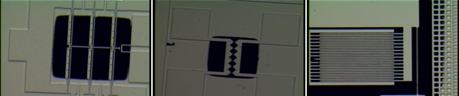 Figure 4 -
Images of MEMS Structures Released on Different Test Chips
Figure 4 -
Images of MEMS Structures Released on Different Test Chips
Mask Making Services
A total of 756 new masks were processed on the pattern
generator in 2008 for our internal (UCB researchers and BMLA), as well as
external customers (other Universities) listed in Marilyn's report.
Special Requests/ other Services
-
Last year, process staff helped one of
the member companies develop their proprietary process. This project stretched
our resources thin, but it was well worth the effort both in terms of the
amount of revenue generated and the opportunity to perform some challenging
process work in the Microlab. Laszlo Petho, our baseline engineer was
intimately involved with this project for the better part of the year. Jimmy lent his time and expertise in the
diffusion and etch area, developing special application processes for this
project. Bob and David Lo worked hard to have different equipment available for
each process step in this project. Marilyn and Kim also helped out with
lithography steps on different iterations of the process flow/development work.
The total amount of staff time/services charged for this project amounted to
$41,828.10.
- Process staff
fabricated few show wafers for Crestec engineers in appreciation of their
installing our new Crestec e-beam lithography system, as well as training staff
on the tool. Process staff also fabricated a show wafer that was presented to
professor King at the end of the year for her six years of mentorship and
support, as a Faculty Director of the Microlab staff supplied the Microlab
office with the regular pocket wafers, as well as poly-Si control wafers for
general use in the Microlab.
VI.
CMOS Baseline activities
Third
Baseline Run (0.35 µm Process)
Last year, the baseline engineer Laszlo Petho,
completed our third 0.35 µm CMOS baseline run (4th six-inch run) initiated by
his predecessor Anita Pongracz. This run (CMOS180) was parked for 6 months due
to the arrival of an important BMLA project in February. Laszlo resumed the
processing work in September was able to complete and test by December. This
run accomplished our main objective of demonstrating the Mix&Match process
on the ASML/GCAWS6 steppers, as well as improved device performance by introducing the shallow trench isolation
in our new fabrication process flow. A
summary report is now available for this run at the following internet link:
http://www.eecs.berkeley.edu/Pubs/TechRpts/2008/EECS-2008-168.html
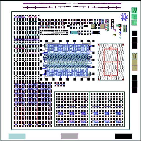
Figure 5 - Baseline CMOS180 Test Chip
VII.
REPORTS,
PUBLICATION, & TRAINING
- Last year I
attended some of the free CAL PACT classes offered on campus. This
included one day Advanced Excel, and Power Point Fundamentals, and a basic
two days Dreamweaver CS3 class on web design.
- A summary report
compiled on the third and the final Plastically Self-Aligned
Micro-Mirrors run R4119 for the MEMS-Exchange program.
- The third 0.35 µm
baseline report was submitted (CMOS180) by Laszlo Petho and Anita Pongracz
in December 2008.
- Process staff
attended BSAC IAB seminars In March and September of 2008 (1/2 day).
- Process staff
attended the Semicon West exhibition in July 2008.
- Process staff attended the Solid State
Technology and Devices Seminars on Fridays.